Our Technology
Our metasurface (or metalens) technology is a game-changer for the optical industry. From invention in the Capasso lab at Harvard, to high volume production ready in the semiconductor foundry, Metalenz is enabling proliferation of compact advanced sensing in mobile and beyond.

Multifunctional optical performance in a single semiconductor layer.
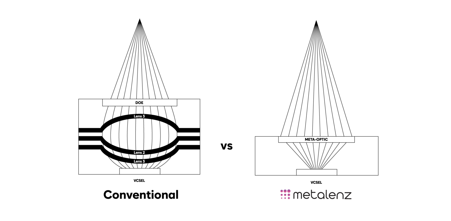
Our breakthrough metalens technology removes complexity, reduces footprint, delivers high performance, and combines up to five optical functions in one single meta-optic.
In 3D sensing modules, accurate transmission and reception of laser light is highly correlated to the precision and performance of the optics used – both for the infrared (IR) laser that emits light and the image sensor that receives and measures it.
In 3D sensing modules, accurate transmission and reception of laser light is highly correlated to the precision and performance of the optics used – both for the infrared (IR) laser that emits light and the image sensor that receives and measures it.
With advantages on both the Tx and Rx side of systems, metalenses enable next-generation 3D sensing capability with significantly improved laser light pattern performance and precision compared to conventional optics.
The level of accuracy and control combined with multifunctional capability in a single surface results in a compact, optically stable module ideal for device miniaturization.
The level of accuracy and control combined with multifunctional capability in a single surface results in a compact, optically stable module ideal for device miniaturization.


Moving Optics into the Semiconductor Foundry
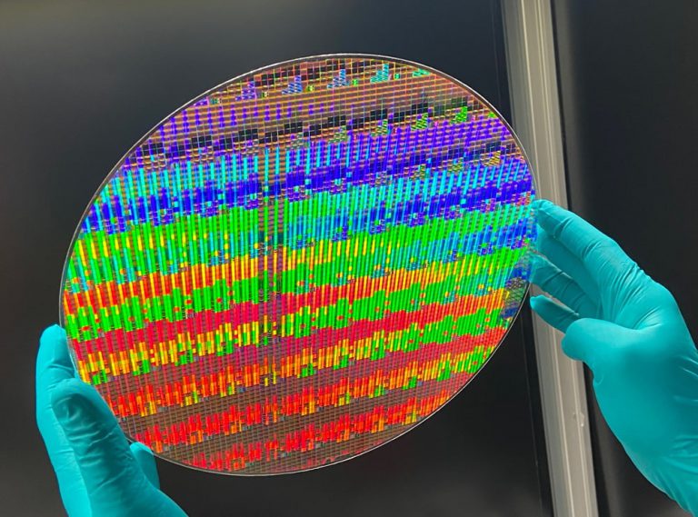
The process of manufacturing metalenses has major advantages. They can be made with a single mask layer with existing semiconductor equipment—producing optics alongside electronics for the first time. Bringing optics manufacturing into the semiconductor foundry consolidates the supply chain, bringing with it cost savings and an entirely new way to assemble thousands of cameras in parallel.

Polar <span>ID</span> Secure Face Unlock for Mobile
PolarEyes Polarization Imaging System
Orion Pattern Projectors
Our Process
Meta-optics designed to your specifications, optimized for manufacturing at scale. The success of metasurface optics relies on precise engineering of the scattering properties of the surface nanostructures, resulting in unprecedented control over electromagnetic radiation with a single layer of material. As a fabless company, we are able to focus our efforts on creating in-house design tools that optimize the full process end to end, from design, to R&D and metrology.
Partner with Us 
Built on foundational research from the Capasso Lab at Harvard University
Built on foundational research from the Capasso Lab at Harvard University
More About Us
Metalenz emerged out of stealth in 2021 to become the first company to commercialize optical metasurfaces.
Marking the beginning of this revolutionary optical technology in real-world devices, meta-optics designed by Metalenz appeared in consumer devices for the first time in 2022 in a range of time-of-flight applications in different consumer devices.
