Metalenz Launches Gemini™ to Make 3D Sensing Easier with Selectable Illuminator Optics
Metalenz Launches Gemini™ to Make 3D Sensing Easier with Selectable Illuminator Optics
Boston, MA, Jan. 24, 2022 – Metalenz Inc., the pioneer in metasurface design and commercialization, today unveiled the Gemini product family, switchable illumination optics based on foundational polarization IP. With a single meta-optic, the Gemini products offer simple, dynamic illumination to address more applications through electronically toggling of optimized illumination patterns – something that is not possible with current refractive lenses and diffractive element optical stacks.
With Gemini, designers can optimize the illumination performance for multiple patterns and toggle between them using Metalenz’s polarization technology.
Metalenz has also announced a recent collaboration with Trumpf to demonstrate switchable illumination modules with Metalenz’s multifunctional-optic and Trumpf’s polarization addressable VCSELs.
Today, mobile phone makers make compromises to balance industrial design, battery usage and user experiences. Features like short-range computational photography and long-range augmented reality require contrasting trade-offs that create a non-optimal solution. These sacrifices to resolution and battery life result in depth sensing solutions that are limited in breadth of applications.
Metalenz’s patented Gemini product line enhances compact and low-cost depth sensing systems, and is set to replace current 3D illumination configurations because of its advantages:
Two illumination patterns with a single optic and VCSEL
Switchable for best of both worlds
2X smaller footprint than discrete alternatives
“Our meta-optic technology allows more control than has been available with the existing commercially available optical toolbox. We have complete control of the intensity of light, the phase of light, and the polarization of light,” said Metalenz co-founder and CEO Rob Devlin. “Depth sensing proliferation has suffered due to the limitations of current optics. Now we have unlocked more applications with a single optic to catalyze 3D sensing to all smartphones.”
Depth sensing proliferation has suffered due to the limitations of current optics. Now we have unlocked more applications with a single optic to catalyze 3D sensing to all smartphones.
Rob Devlin, Metalenz Co-founder and CEO
3D depth sensing works by illuminating a scene with infrared light and determining the distances of the object(s) using the reflected light collected on a special image sensor. Depth sensing on smartphones is optimized based on the distance of the object in the scene or the application. For computational photography and many social media applications, the objects of interest are less than 5 meters away from the camera. They benefit from flood illumination that will help capture high detail and edge resolution. In contrast, augmented reality applications can extend to 10 meters and beyond. Illumination by dot projectors permits higher sensing integrity at longer distances and maintains a power budget in line with immersive user experience requirements of mobile devices.
Metalenz’s proprietary technology uses single meta-optics to project thousands of high-intensity dots of light in one mode and a flood of light in the second mode. Instead of compromising system performance or going without 3D imaging, Gemini™ eliminates the trade-off. Designers can optimize the illumination performance for multiple patterns and toggle between them using Metalenz’s polarization technology.
Already engaged with a number of the world’s largest manufacturers including a recent foundry partnership with STMicroelectronics, Metalenz has the partners and supply chain logistics to meet the scale of OEMs across consumer and automotive industries. The company’s simplified manufacturing process consolidates the optics and sensor supply chain (producing both at one facility), resulting in meta-optic lenses that are more cost-efficient and compact than conventional lenses to meet the rapid increase in cameras and sensing devices.
Metalenz is backed by semiconductor leaders including 3M Ventures, Intel Capital, and TDK Ventures. To partner with or learn more about how Metalenz is revolutionizing optical sensing in consumer electronics and beyond, visit: metalenz.com.
About Metalenz
Metalenz, founded in 2016, is the first company to commercialize meta-optics. Our meta-surface technology provides complex, multifunctional optical performance in a single semiconductor layer and enables moving large-scale production of optics into semiconductor foundries—printing lenses like computer chips. As a fabless semiconductor company, Metalenz is focused on the design and unique applications of meta-optics, transforming sensing across consumer, healthcare, and automotive applications.
The company has the exclusive worldwide license to the portfolio of foundational intellectual property relating to metasurfaces developed in the Capasso Lab at Harvard University and has more than 20 patents on innovations that simplify and improve optical devices across multiple markets.
Metalenz Unveils PolarEyes: The First Polarization Technology Designed to Increase Your Security and Manage Healthcare From Smartphones
Metalenz Unveils PolarEyes: The First Polarization Technology Designed to Increase Your Security and Manage Healthcare From Smartphones
The Harvard-born meta-optics company brings polarized lenses to consumer and mobile devices for improved privacy and security features, at-home healthcare, and air quality detection tools.
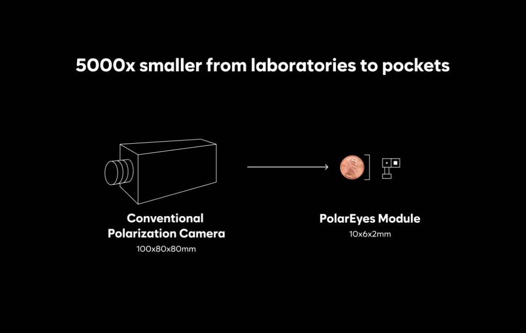
Boston, Jan. 20, 2022 — Metalenz, the first company to commercialize meta-optics, today unveils PolarEyes: a new polarization technology that brings entirely new forms of sensing to camera-equipped devices. Built on foundational research from the Capasso Lab at Harvard University, Metalenz’s latest lenses enable advanced optical sensing to improve privacy features, alert drivers to safety hazards on the road, and make at-home healthcare more accessible. The full-stack, system-level solution combines physics and optics, software and hardware to power everything from next-generation smartphones and consumer electronics, to new healthcare and automotive applications.
“Our technology acts as a second set of eyes in very vulnerable situations. This could be a virtual visit to the dermatologist, or protecting the security of our mobile devices,” said Robert Devlin, co-founder and CEO of Metalenz. “Advanced optics capabilities are crucial to understanding our surroundings but typically reserved for science-grade labs. With PolarEyes, we are putting this power into people’s pockets for the first time, transforming the way they see and interact with the world.”
Powering the future of optical sensing in today’s cameras
Consumers are increasingly reliant on their camera-equipped devices. Telehealth usage has increased 38X from pre-COVID baseline, for example, as patients and providers sought ways to safely access and deliver healthcare. But as the demands on our hardware increase, lenses have lagged behind. Metalenz PolarEyes collects the polarized light information traditional cameras discard and parses through that information to better interpret the world around us.
PolarEyes unveils information and unlocks features never-before-available at a mobile form factor and price point enabling:
Spoof-Proof Facial Authentication: Provides correct identification of users versusfacial-spoofing masks and photos to safeguard consumer devices against fraudsters.
Enhanced 3D Sensing: Provides more details to detect shapes and edges with increased contrast; improving virtual backgrounds’ quality and 3D object scanning resolution in AR/VR environments.
Material Classification: Identifies molecular makeup of objects, giving automakers the ability to alert drivers to road hazards like black ice, and doctors the potential to diagnose skin cancer from a smartphone.
Anti-glare Vision: Works around glare, the reflective light which often overpowers vision and machine vision, enabling robots to better maneuver and automobiles the ability to monitor for distracted driving – a new safety measure required in all vehicles by 2025.
Already engaged with a number of the world’s largest manufacturers including a recent foundry partnership with STMicroelectronics, Metalenz has the partners and supply chain logistics to meet the scale of OEMs across consumer and automotive industries. The company’s simplified manufacturing process consolidates the optics and sensor supply chain (producing both at one facility), resulting in meta-optic lenses that are more cost-efficient and compact than conventional lenses to meet the rapid increase in cameras and sensing devices.
Metalenz is backed by semiconductor leaders including 3M Ventures, Intel Capital, and TDK Ventures. To partner with or learn more about how Metalenz is revolutionizing optical sensing in consumer electronics and beyond, visit: metalenz.com.
About Metalenz
Metalenz, founded in 2016, is the first company to commercialize meta-optics. Our meta-surface technology provides complex, multifunctional optical performance in a single semiconductor layer and enables moving large-scale production of optics into semiconductor foundries—printing lenses like computer chips. As a fabless semiconductor company, Metalenz is focused on the design and unique applications of meta-optics, transforming sensing across consumer, healthcare, and automotive applications.
The company has the exclusive worldwide license to the portfolio of foundational intellectual property relating to metasurfaces developed in the Capasso Lab at Harvard University and has more than 20 patents on innovations that simplify and improve optical devices across multiple markets.
Metalenz partners with STMicroelectronics to develop manufacturing processes
STMicroelectronics and Metalenz Partner to Transform Optical Sensing for Consumer, Automotive, and Industrial Applications
• Agreement encompasses development of manufacturing processes, industrialization of meta-surface optics, and technology licensing.
• Revolutionary flat-lens technology brings performance, power, size, and cost advantages to complex optical system
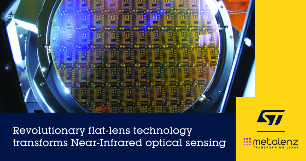
Geneva, Switzerland; and Boston, MA, USA – June 2, 2021 — STMicroelectronics (NYSE: STM), a global semiconductor leader serving customers across the spectrum of electronics applications, and Metalenz Inc., the pioneer in meta-surface design and commercialization, today announced a co-development and license agreement that will see ST develop manufacturing processes for Metalenz’s meta-optics technology for next-generation smartphones, consumer devices, healthcare, and automotive applications. Metalenz is a spin-out of the group of Federico Capasso at Harvard University, where the technology was invented. This breakthrough technology is expected to be ready for mass production by the end of this year.
Metalenz’s multifunctional meta-surface optics enable new forms of sensing for the next generation of smartphones and other consumer devices, as well as healthcare and automotive applications. For example a camera built around this new flat-lens technology can collect more light for brighter images and produce images of the same or better quality than traditional refractive lenses while consuming less power and taking up less space.
ST will integrate Metalenz’s meta-surface optics technology into ST’s existing diffractive optics manufacturing process at its 300mm wafer fab in Crolles, France, leveraging ST’s position at the forefront of the fast-growing Near-Infrared (NIR) optical sensing market. Today ST leads the market for time-of-flight (ToF) proximity and distance sensors with over 1 billion devices shipped to customers.
Eric Aussedat, Executive Vice President & General Manager of ST’s Imaging Division, said, “With its advantages in power, efficiency, and performance, multifunctional optics technology can be a game changer for the next generation of optical sensors used in smartphones and other consumer devices, as well as healthcare and automotive applications. In combining Metalenz’s advances with our proprietary technology, manufactured in our state-of-the-art 300mm production facility in Crolles,this partnership will support ST’s continued offering of the most innovative and advanced optical-sensing solutions to its customers.”
“We are thrilled to be working with an industry leader like ST. The technology developed by Metalenz is a perfect complement to ST’s advanced capabilities and market position,” said Dr. Rob Devlin, CEO and co-founder of Metalenz. “We adopted a fabless business model so that we can focus on the innovation and design of revolutionary optics to transform sensing from smartphones to automobiles. Working with ST enables us to expand our product offering while leveraging ST’s high-volume fabrication capability and enables ST’s already differentiated product lines to reach new heights with Metalenz inside.”
The technology used in today’s smartphones is changing and developing at a very fast rate to squeeze more and better functionality into less space. Still, the lenses remain essentially unchanged since medieval times. That’s now changing, with meta-surface optics introducing a new breed of lens, which works on very different fundamental principles. Instead of using bulkier curved surfaces, meta-surface optics combine multiple complex optical functions in a single flat layer. This shrinks the size of each lens element while also cutting the number of lens elements needed, dramatically reducing the size of the optical lens, the number of components, the complexity of assembly, and the overall cost.
The technology developed by Metalenz is a perfect complement to ST’s advanced capabilities. Combining semiconductor manufacturing and optics, ST will use advanced lithographic masks to build tunable diffractive-wavefront layers on a meta-surface in a semiconductor wafer fab. Like silicon ICs, the flat meta-surface lenses are processed in a semiconductor clean room using the same manufacturing technology. The lenses will feature nanostructures one-thousandth the width of a human hair. These nanostructures appropriately bend light rays to realize in a single layer the same functionality as a complex multi-element refractive lens system.
This technology is initially targeted at the fast-growing NIR market. NIR wavelengths are used in all the 3D sensing functions, such as face identification, autofocus assist, mini-LIDAR, and AR/VR depth mapping, that are becoming standard in today’s smartphone. Given the benefits, optical lenses made in a semiconductor wafer fab could someday be as common as traditional refractive lenses.
About STMicroelectronics
At ST, we are 46,000 creators and makers of semiconductor technologies mastering the semiconductor supply chain with state-of-the-art manufacturing facilities. An independent device manufacturer, we work with more than 100,000 customers and thousands of partners to design and build products, solutions, and ecosystems that address their challenges and opportunities, and the need to support a more sustainable world. Our technologies enable smarter mobility, more efficient power and energy management, and the wide-scale deployment of the Internet of Things and 5G technology. Further information can be found at www.st.com.
About Metalenz
Metalenz, founded in 2016, is the first company to commercialize meta-optics. Our meta-surface technology provides complex, multifunctional optical performance in a single semiconductor layer and enables moving large-scale production of optics into semiconductor foundries—printing lenses like computer chips. As a fabless semiconductor company, Metalenz is focused on the design and unique applications of meta-optics, transforming sensing across consumer, healthcare, and automotive applications.
The company has the exclusive worldwide license to the portfolio of foundational intellectual property relating to metasurfaces developed in the Capasso Lab at Harvard University and has more than 20 patents on innovations that simplify and improve optical devices across multiple markets. For more information, please visit https://www.metalenz.com/
Metalenz Launches Orion™, the World’s Simplest, Most Compact Dot Pattern Projector.
Metalenz Launches Orion™, the World’s Simplest, Most Compact Dot Pattern Projector.
• Metalenz’s simpler dot projectors enable 3D sensing to proliferate to all smartphones.
• Metalenz has secured high volume manufacturing partnerships and has customers in the queue, with broad availability of evaluation kits in June.
Boston, MA, May 26 2021 : Metalenz Inc., the pioneer in metasurface design and commercialization, today unveiled the OrionTM product family, the world’s simplest, high performance dot pattern projectors. Current dot pattern projectors, used in mobile devices for features like facial recognition and 3D sensing, have been a logistic and aesthetic headache for cell phone manufactures–eating up valuable space, interrupting the phone display and requiring complex assembly of many different components.
Using its patented metasurface technology, the Orion product family is a simplified and more efficient solution that is bound to displace refractive lens and diffractive element optical stacks with a single meta-optic. “If you look at dot pattern projectors in cell phones today, these are some of the most complex and bulky modules in the phone.” said Robert Devlin, co-founder/CEO, Metalenz. “The size, complexity and cost has limited 3D sensing and face unlock to just the top tier cell phone companies. What Metalenz provides with our meta-optic technology is the simplest possible approach. We’re able to improve the system level performance while replacing as many as six optics in the current modules with a single meta-optic. This results in a size reduction in all three dimensions. Ultimately, the Orion product line will enable under-display sensing and allow much broader adoption of 3D sensing and face unlock features across all cell phones.”
Metalenz’s patented Orion pattern projector product line is set to replace current 3D optical configurations in smartphones because of its advantages:
● Simpler – replaces as many as six optical parts in an illumination system (refractive lenses, mirrors, DOE) with a single meta-optic piece.
● Smaller – collapses form factor to fit in the tightest of spaces, hiding under screens or in the tiniest of nooks in a phone.
● Brighter – light projected to where it is needed the most for high resolution constellations or out far out distances, balancing performance and power savings.
● Better – architecture drastically lowers assembly complexity and cost to drive more depth sensing sockets for user authentication and AR.
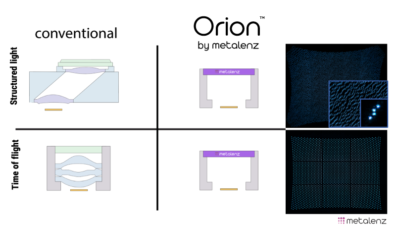
The advantages of Orion products extend to both structured light (SL) and time of flight (ToF) 3D depth sensing solutions. The meta-optics improve system level signal-to-noise-ratio, resulting in better performance in sunlight, higher resolution, longer sensing distances, and improved battery life.
The Orion 50, the highest dot density product in the family, boasts more than 50,000 projected dots with an optical module height thin enough for the most advanced mobile devices. It radically simplifies what has traditionally been a six element stack (four refractive lenses, mirrors to achieve a folded optical path, and a DOE) into one single meta-optic system. Orion 50 means component reduction, tiny size, performance we are accustomed to, and dramatically easier manufacturing. This simplification will enable more phone makers to put sensors and cameras beneath a device’s glass display and ultimately in the palms of our hands.
On the flip side, smartphones with world-facing (a.k.a the back of the phone) 3D depth sensing cameras deliver professional looking photography effects like bokeh and are enabling emerging AR applications. Depth sensing cameras rely on active illumination of the scene with lasers and capture of reflected light with specialized ToF sensors. Illuminating brighter to cover greater distances and flooding the scene for long periods of time can be a major drain on a phone’s battery life. These are the antithesis of bringing forth more immersive and encompassing AR applications.
Orion 2.5 projects 2,500 high intensity dots into the scene so more light will travel the distance back to the image sensor. High resolution depth information is made possible at distances of 10 meters or more. Orion 2.5 conserves power and enables a new arena for AR in smartphones, head mounted displays, and consumer electronics. It stays true to the Orion family roots – simpler, brighter, better optics – while doing away with system complexity and driving down the barriers for integration and board adoption.
About Metalenz Metalenz, founded in 2016 is the first company to commercialize meta-optics. The company is backed by leading investors including 3M, Applied Ventures LLC, Intel Capital, M Ventures and TDK Ventures. The company has the exclusive worldwide license to the portfolio of foundational intellectual property relating to metasurfaces developed in the Capasso Lab at Harvard University and has more than 20 patents on innovations that simplify and improve optical devices across multiple markets. Recently featured in TechCrunch, Wired, The New York Times, and Forbes.
With its recent flat-lens technological achievements, manufacturing partnerships in place, and growing customer list, Metalenz is poised to revolutionize sensing in smartphones and consumer electronics.
Metalenz Launches with $10M from 3M, Applied Ventures, Intel Capital, M Ventures, and TDK to Power the Next Generation of Smartphone Sensors
Metalenz Launches with $10M from 3M, Applied Ventures, Intel Capital, M Ventures, and TDK to Power the Next Generation of Smartphone Sensors
Startup Pioneering New Microchip Lens with Structures 1000x Smaller than a Human Hair Partners with Consumer Electronic Giants to Revolutionize Mobile Device Sensors
Boston, MA – Thursday, February 4, 2021 : Metalenz, the first company to commercialize meta-optics, today officially launched out of stealth and announced it has raised $10 million from 3M Ventures, Applied Ventures LLC, Intel Capital, M Ventures and TDK Ventures, along with Tsingyuan Ventures and Braemar Energy Ventures. The new investment allows Metalenz to scale production and accelerate the development of miniature optics on a chip technology and its radically new lens that will power the next generation of sensors for use in smartphones and other consumer, healthcare, and automotive applications.
Commercializing meta-optic technology pioneered at Harvard John A. Paulson School of Engineering and Applied Sciences (SEAS), Metalenz was co-founded by Robert Devlin, PhD, and professor of applied physics Federico Capasso, PhD. With a decade of research behind it and 15 issued patents on the concept, the company has an intellectual property head start and is already engaged with a number of the world’s largest manufacturers in the consumer electronics and automotive spaces, from OEMs to subsystem makers.
“Over the past 20 years, most of the advances in camera and sensing technology in consumer electronics has been to electronics and algorithms but the optics themselves have remained relatively unchanged. At Metalenz we’re providing new functionality to lenses that enable large-scale production in the same semiconductor foundries making the electronics for the first time,” said Rob Devlin, co-founder and CEO of Metalenz. “We’re thrilled to welcome tier 1 semiconductor leaders as investment partners as we bring entirely new forms of sensing to consumer electronics that will eventually revolutionize everything from automotive and healthcare industries to phones, augmented reality, and deskless workforces.”
A Flat Lens with Structures 1000x Smaller than a Human Hair Poised to Revolutionize Mobile Devices
Despite the improvements in cameras, lens technology has remained relatively unchanged for hundreds of years. The emerging field of meta-optics, or optical metasurfaces, centers on engineered materials with patterned structures 1000x smaller than a human hair specifically designed to exploit properties that cannot be obtained from bulk natural materials.
Unique meta-optic properties permit the combination of several lenses into a single, thin, and flat surface and unlock new possibilities including improved 3D sensing and new sensors that can fit under the display of a cell phone. The result is lenses that enable a brighter, higher quality infrared picture than conventional lenses are able to produce. For consumers, this means more powerful phone capabilities that can help them snap more professional looking pictures, even in the most challenging environments, while promoting longer battery life.
“Metalenz is pioneering a lens that is thinner, lighter, and far less complex than other lens solutions, by leveraging an incredibly unique and transformative materials technology which is grounded in years of scientific research,” said Andrew Maywah, Investment Director at TDK Ventures. “TDK is excited to partner with Metalenz and apply its ecosystem and technology expertise in optical sensing and actuation to further innovate on lens solutions that will have a major impact on cameras and illuminators in smartphones, cameras, and laptops worldwide.”
“Applied Ventures is excited to continue its support of the Metalenz team as part of our growing portfolio of companies spanning Materials to Systems™. Applied’s broad materials engineering capabilities can help Metalenz continue advancing its disruptive flat optical technology that allows for advanced manipulation of light and the potential to combine multiple refractive lenses into a single stack,” said Jaclyn Kossman, Senior Investment Manager at Applied Ventures.
Metalenz holds an exclusive worldwide license, through Harvard University’s Office of Technology Development, to a portfolio of foundational intellectual property relating to metasurfaces developed in the Capasso Lab at Harvard SEAS.
As a fabless semiconductor company, Metalenz is able to focus resources on engineering and development, allowing for a quick ramp-up in production of its meta-optics to meet market demands of fast, high volume consumer electronics companies, scaling to produce millions of high quality units quickly, while keeping production costs down.
“TDK is excited to partner with Metalenz and apply its ecosystem and technology expertise in optical sensing and actuation to further innovate on lens solutions that will have a major impact on cameras and illuminators in smartphones, cameras, and laptops worldwide.”