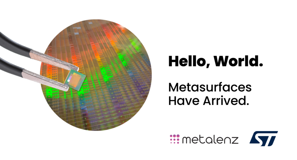
Metalenz Confirms Samsung ISOCELL Vizion Image Sensor as Light- Engine for Polar ID, the World’s Smallest, Most Affordable and Secure Face Unlock Solution.
Metalenz Confirms Samsung ISOCELL Vizion Image Sensor as Light- Engine for Polar ID, the World's Smallest, Most Affordable and Secure Face Unlock Solution.
Metalenz chose Samsung’s new high-performance global-shutter NIR image sensor, the ISOCELL Vizion 931, as light-engine for its revolutionary polarization-sorting imaging system.
Collaboration pairs industry-leading image sensor capabilities of ISOCELL Vizion 931 with Metalenz groundbreaking ability to sort light based on the state of its polarization.
Polar ID leverages the unique polarization signature of the human face to create the world’s smallest, most affordable, and secure biometric face unlock solution for smartphones.
The proven performance and manufacturing scale of Samsung’s semiconductor business brings instant high-volume supply capabilities Polar ID production that can meet the requirements of even the largest OEMs.
February 26, 2024, Barcelona, Spain – Meta-optics industry leader Metalenz announced today that it has chosen Samsung Electronics’ ISOCELL Vizion 931 as image sensor for Polar ID, the world’s only consumer-grade imaging system that can sense the full polarization state of light. Unlike other facial biometric solutions that require multiple different images to work, the polarization signature of a human face enables the fast and secure recognition and authentication from a single Polar ID image. The powerful simplicity of Polar ID enables a 50% size and cost reduction over traditional face unlock solutions, and partnership with Samsung provides industry leading image sensor performance and manufacturing scale to drive rapid smartphone adoption.
“Our collaboration with Metalenz is not just about combining technologies; it marks a pivotal advancement in biometric imaging capabilities, making face unlock solutions with enhanced security and affordability accessible on a global scale,” said CY Lee, Vice President of the Sensor Sales & Marketing Team at Samsung Electronics. “We are energized to collaborate with Metalenz, a company that shares our commitment to bringing visionary solutions to market.”
“Polar ID is poised to bring secure face unlock to hundreds of millions of phones and a whole new class of sensing to millions of people. Leveraging the performance and scale of Samsung’s ISOCELL Vizion 931 image sensor allows our Polar ID cameras to quickly and efficiently determine the polarization information in a scene, from which our imaging algorithms and machine learning models authenticate the Polar ID images,” said Rob Devlin, Metalenz CEO and co-founder. “The collaboration with Samsung marks a new era for mobile vision systems and provides Metalenz with a partner that has the proven quality and scale required to bring Polar ID to all phones.”
Within the Polar ID system, Metalenz’ breakthrough polarization-sensitive meta-optic is combined with a derivative of the new ISOCELL Vizion 931 image sensor. Coupled with Metalenz technology, the same light-engine that is used in the ISOCELL Vizion 931 can now capture polarized images in the near infrared spectrum with industry-leading quantum efficiency and advanced global shutter technology, allowing Polar ID cameras to enable the next generation of biometric imaging.
Polar ID cameras will make their public debut at MWC 2024 in Barcelona, where Metalenz will showcase the speed, security, compact footprint, and unparalleled affordability of this new face unlock solution integrated into a smartphone reference design powered by the new Snapdragon® 8 Gen 3 Mobile Platform.
Polar ID is under early evaluation with several leading smartphone OEMs. Additional evaluation kits will be made available in Q2 2024. OEMs looking to schedule a live demo with Metalenz at MWC Barcelona can email sales@metalenz.com to schedule.
About Metalenz: Metalenz is at the forefront of driving innovation in optics with metasurface technology, providing solutions that redefine the possibilities of mobile imaging and sensing. Metalenz is the first company to bring metasurfaces to mass markets, with millions of its meta-optics already integrated in consumer devices, combining the functionality of three or four complex lenses and components into a single flat device, mass produced in existing semiconductor foundries. The company’s first full system solution, Polar ID, is a groundbreaking, ultra-secure, small, and affordable face unlock solution for mobile that harnesses the unique polarized light sorting capabilities of metasurfaces, enables mobile devices to see beyond the limits of current visual systems.
About Samsung ISOCELL Vizion 931: Designed in a one-to-one ratio VGA resolution (640 x 640) that packs more pixels in a smaller form factor, the ISOCELL Vizion 931 is optimal for eye tracking as well as facial and gesture detection in imaging solutions utilizing near-infrared illumination at 850nm or 940nm. The ISOCELL Vizion 931 also achieves the industry’s highest level of quantum efficiency, delivering an impressive 60% at 850nm infrared light wavelength and 38% at 940nm. This feat was made possible by incorporating Front Deep Trench Isolation (FDTI) which places an insulation layer between pixels to maximize light absorption, in addition to the backside scattering technology (BST) that enhances light absorption.
Metalenz has been commercializing its metasurface technology since 2016. The Company’s “meta-optics” allow complex optical sensing solutions previously confined to scientific or medical labs, to be shrunk to a size and price point compatible with mobile. The tech company does this by combining the functionality of three or four complex lenses and components into a single flat device. Unlike traditional lenses, these optics are mass produced in existing semiconductor foundries—essentially printed like computer chips. Already in mass production and integrated in consumer devices with dot pattern projectors for facial recognition and lenses for 3D sensing, Metalenz is the first company to bring metasurfaces to mass markets.
Qualcomm, Snapdragon, Hexagon, and Spectra are trademarks of Qualcomm Incorporated, registered in the United States or other counties.
Snapdragon, Qualcomm Hexagon, and Qualcomm Spectra are products of Qualcomm Technologies, Inc.
Press inquiries
media@metalenz.com
Media coverage
02|15|2024
Get ready to be submerged by the new optics revolution – An interview with Metalenz
Metalenz Raises $30 Million Series B Led by Neotribe Ventures
Metalenz Raises $30 Million Series B Led by Neotribe Ventures
October 12, 2022, Boston, MA – Metalenz, the market leader for metasurface optics for high-performance 3D sensing solutions, today announced the closing of a $30M Series B, led by Neotribe Ventures. The funding will be used to meet the growing demand for the company’s existing 3D Sensor metasurface optics while simultaneously accelerating the market introduction of its revolutionary new polarization sensing solution, PolarEyes. The round also saw participation from Foothill Ventures, M Ventures, Intel Capital, Osage University Partners, TDK Ventures, 3M Ventures, Global Brain, SG Innovate, Hegemon Capital, and Braemar Energy Ventures.
“When we launched our first products as the key enabler for simpler, next generation 3D ToF products earlier this year, we proved that the performance of our metasurface optics is unparalleled in the 3D sensing market, and that our new technology can reach end-users at a massive scale,” said Metalenz co-founder and CEO Rob Devlin. “Since then, demand has dramatically increased, and the oversubscribed round is a testament to how our metasurface optics can completely transform the way people and machines interact with and understand the world around them. Going forward we are particularly excited to benefit from the deep knowledge and vast network of our lead investor in the Series B, Neotribe Ventures.”
“At Neotribe we are focused on investing in companies that are solving really hard technical problems that disrupt non-traditional industry sectors,” said Kittu Kolluri, Founder and Managing Director of Neotribe Ventures. “Metalenz represents the perfect blend of a disruptive deep tech solution being applied to a large and innovation-starved market, optics. We look forward to supporting Rob and his team as they scale the company and product roadmap to address this multi-billion-dollar opportunity.”
“Metalenz represents the perfect blend of a disruptive deep tech solution being applied to a large and innovation-starved market, optics. We look forward to supporting Rob and his team as they scale the company and product roadmap to address this multi-billion-dollar opportunity.”
– Kittu Kolluri, Founder and Managing Director of Neotribe Ventures
About Metalenz
Founded in 2016 and the first to commercialize meta-optics, Metalenz is enabling the next generation of 3D sensing in consumer electronics, automotive and industrial robotics markets. Built on research from the Capasso Lab at Harvard University, with exclusive worldwide license to foundational IP relating to metasurfaces, Metalenz has 20+ patents on innovations that simplify and improve optical devices. Unlike traditional optics, the company’s metasurface technology provides complex, multifunctional optical performance in a single semiconductor layer, relocating large-scale production of optics to semiconductor foundries—printing lenses like computer chips. Metalenz launched out of stealth in 2021 with funding from leading investors including 3M Ventures, Applied Ventures LLC, Intel Capital, M Ventures, TDK Ventures, and Foothill Ventures. Now in market, Metalenz metasurface optics will be in millions of consumer devices this year.
To learn more about how Metalenz is revolutionizing optical sensing in consumer electronics and beyond, contact sales@metalenz.com
About Neotribe Ventures
Neotribe Ventures focuses on strategic investments in early to growth-stage companies developing breakthrough technologies that stretch the imagination. Founded in 2017, the firm manages nearly $450 million in assets across three funds and has invested in a diverse set of companies including computational biology, enterprise security and infrastructure, robotics and AI, blockchain technologies, cleantech, and more. Just as tribes represent small, protective, and caring groups, Neotribe believes that startups with innovative and aspirational teams thrive if provided the security and backing to be unafraid in the pursuit of new ideas, excellence, and success.
To learn more about how Neotribe is partnering with entrepreneurs in the U.S., Europe, Israel, India, and Australia in their quest to solve complex and deeply impactful problems to create lasting change, visit www.neotribe.vc.
Metalenz Receives Platinum 2022 Laser Focus World Innovator Award
PolarEyes™ Receives Platinum Level Innovation Award
PolarEyes™ Receives Platinum Level Innovation Award
Metalenz, the first company to commercialize metasurface optics, announced today that its polarization sensing technology, “PolarEyes™”was recognized with the highest honor by the 2022 Laser Focus World Innovators Awards. An esteemed and experienced panel of judges from the optics and photonics community recognized Metalenz as a Platinum honoree.
“On behalf of the Laser Focus World Innovators Awards, I would like to congratulate Metalenz on their Platinum level honoree status,” said Laser Focus Word Editor-in-Chief Peter Fretty. “This competitive program allows Laser Focus World to celebrate and recognize the most innovative products impacting the photonics community this year.”
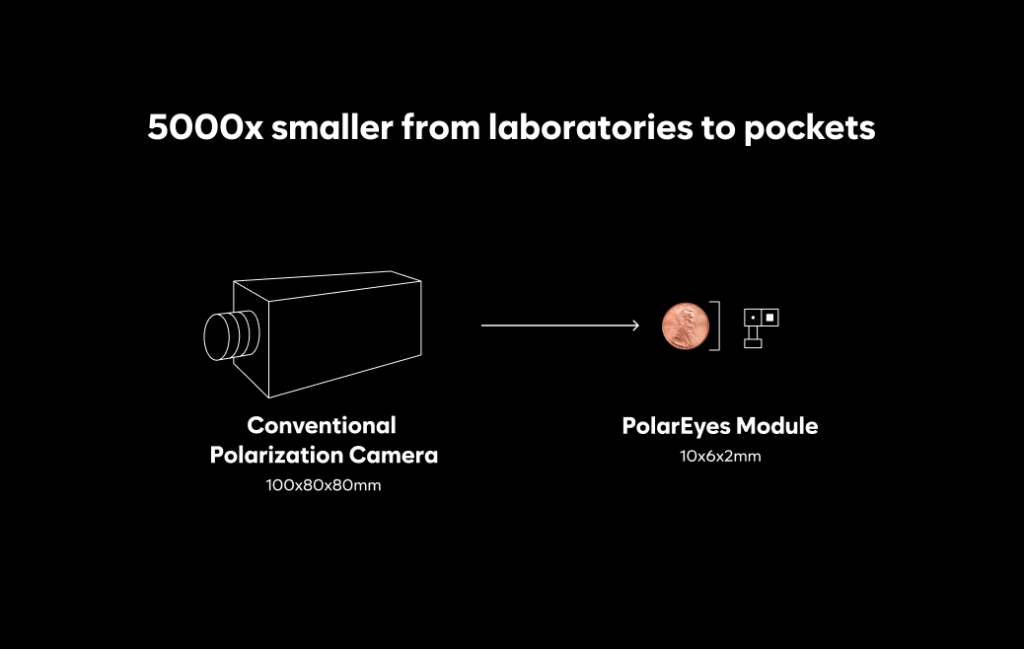
PolarEyes is the next generation of 3D sensing. Using a single metasurface optic paired with an image sensor, PolarEyes works to distinguish objects by way of polarized light, providing much more detailed information about a scene, including increased shape contrast and molecular makeup of objects. Shrinking a full-stokes polarization sensor by over 5000x, the module unlocks a host of sensing capabilities never-before-available at a mobile form factor-from more secure facial recognition in smartphones and consumer electronics, to new healthcare and automotive applications.
“By interpreting polarization information in light with a single optic, PolarEyes can provide a whole new information set to mass applications. In the era of AI and machine vision, these systems make increasingly more decisions that impact our lives. By providing a new, more complete information set to these systems, algorithms can be more efficient and their decisions more accurate.” Said Metalenz co-founder and CEO Rob Devlin. “Starting from a fundamental innovation by Dr. Noah Rubin while he was in Federico Capasso’s group, Metalenz is now poised to deliver this technology to real world modules with PolarEyes.”
“This competitive program allows Laser Focus World to celebrate and recognize the most innovative products impacting the photonics community this year.”
Peter Fretty, Laser Focus World Editor-in-Chief
About Laser Focus World
Published since 1965, Laser Focus World has become the most trusted global resource for engineers, researchers, scientists, and technical professionals by providing comprehensive coverage of photonics technologies, applications, and markets. Laser Focus World reports on and analyzes the latest developments and significant trends in both the technology and business of photonics worldwide — and offers greater technical depth than any other publication in the field.
About Metalenz
Metalenz, founded in 2016, is the first company to commercialize meta-optics. With exclusive worldwide license to the portfolio of foundational intellectual property relating to metasurfaces developed in the Capasso Lab at Harvard University, Metalenz has more than 20 patents on innovations that simplify and improve optical devices across multiple markets. The company’s meta-surface technology provides complex, multifunctional optical performance in a single semiconductor layer, relocating large-scale production of optics to semiconductor foundries. Metalenz launched out of stealth in 2021 with funding from leading investors including 3M Ventures, Applied Ventures LLC, Intel Capital, M Ventures, TDK Ventures, and Foothill Ventures. Now in market, Metalenz optics will be in millions of consumer devices this year.
Media Contact : carly.glovinski@metalenz.com
Metalenz Expands Leadership Team in Response to Growing Demand for Its Breakthrough Metasurface Optics
Metalenz Expands Leadership Team in Response to Growing Demand for Its Breakthrough Metasurface Optics
Boston, MA – July 20, 2022 – Metalenz, the first company to commercialize meta-optics, today announces the appointment of Lars Johnsson Vice President of Product, Marketing and Business Development and Hao Zhou as Head of Sales in Asia.
“Having launched our breakthrough meta-optics solution as a key enabler of ST Microelectronics’ next generation 3D ToF products earlier this year, we’ve proven we can reach end-users at a massive scale, and demand has only increased,” said Metalenz co-founder and CEO Rob Devlin. “Now is the time to add the skill and expertise of Lars and Hao to promote our technology in different regions as we launch a direct line of Metalenz near infrared imaging and sensing products.”
Lars will lead all aspects of Metalenz’s product strategy and revenue generation, drawing on over 20 years of repeated success bringing new and disruptive products to market, creating ecosystems for innovative solutions, and growing market share, revenue, and profit ahead of the competition. Prior to Metalenz, Lars was VP of Mobile Marketing at Skyworks Solutions, Sr. Director of Product at TDK, and VP of Marketing and Business Development at Cavendish Kinetics and Beceem Communications.
As Head of Sales in Asia, Hao will use his rich insights and connections in consumer electronics to drive consumer engagement and revenue generation in the Greater China Region. He brings decades of experience in the opto-electronic industry selling advanced optical components, modules, and systems. Prior to joining Metalenz, Hao founded Qtech as General Manager, where he led the effort in pushing TSV technology-based wafer level packaging into mass production and developed one of world’s first cellphone camera modules.
Two new appointees will accelerate the launch of next generation metasurface optics for advanced sensing applications.
About Metalenz
Metalenz, founded in 2016, is the first company to commercialize meta-optics. With exclusive worldwide license to the portfolio of foundational intellectual property relating to metasurfaces developed in the Capasso Lab at Harvard University, Metalenz has more than 20 patents on innovations that simplify and improve optical devices across multiple markets. The company’s metasurface technology provides complex, multifunctional optical performance in a single semiconductor layer, relocating large-scale production of optics to semiconductor foundries—printing lenses like computer chips. Metalenz launched out of stealth in 2021 with funding from leading investors including 3M Ventures, Applied Ventures LLC, Intel Capital, M Ventures, TDK Ventures, and Foothill Ventures. Now in market, Metalenz metasurface optics will be in millions of consumer devices this year. To partner with Metalenz and learn more about how they’re revolutionizing optical sensing in consumer electronics and beyond, contact sales@metalenz.com
Metalenz and STMicroelectronics Deliver World’s First Optical Metasurface Technology for Consumer Electronics Devices.
Metalenz and STMicroelectronics Deliver World’s First Optical Metasurface Technology for Consumer Electronics Devices.
Metalenz metasurfaces are now on the market through its partnership with STMicroelectronics, marking the introduction of this revolutionary optical technology in real-world devices
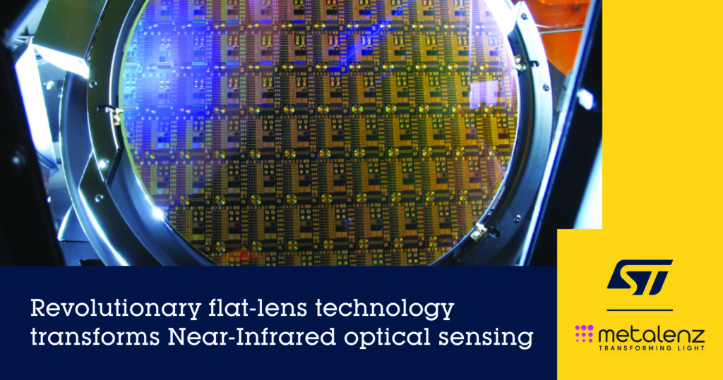
Boston, MA and Geneva, Switzerland – June 9, 2022 – Metalenz, the first company to commercialize meta-optics, and STMicroelectronics (NYSE: STM), a global semiconductor leader serving customers across the spectrum of electronics applications, today announce that ST’s currently released VL53L8 direct Time-of-Flight (dToF) sensor is the highly anticipated market debut of the meta-optics devices developed through their partnership, which was disclosed in June 2021.
Metalenz’s Harvard-born, meta-optics technology can replace existing complex and multi-element lenses and provide additional functionality with a single meta-optic embedded in time-of-flight (ToF) modules from ST, the leading company in supplying 3D sensing modules. The introduction of Metalenz technology in these modules brings performance, power, size, and cost advantages to a multitude of consumer, automotive, and industrial applications. This marks the first time metasurface technology is commercially available and being used in consumer devices.
Unlike traditional molded and curved lenses, Metalenz’s novel optics are completely planar. Planar metasurface optics are now being manufactured on silicon wafers alongside electronics in ST’s semiconductor front-end fabs for the first time. The meta-optics collect more light, provide multiple functions in a single layer, and enable new forms of sensing in smartphones and other devices, while taking up less space. Metalenz’s flat-lens technology replaces certain existing optics in ST’s FlightSense™ ToF modules, which serve applications such as smartphones, drones, robots, and vehicles. In these, ST has sold more than 1.7 billion units to date.
“More than a decade of foundational research has brought us to this point. Market deployment of our meta-optics makes this the first metasurface technology to become commercially available,” said Rob Devlin, co-founder and CEO of Metalenz. “ST’s technology, manufacturing expertise, and global reach allow us to impact millions of consumers. We have multiple wins that mark the first application of our platform technology and we are now designing entire systems around its unique functionality. Our meta-optics enable exciting new markets and new sensing capabilities in mobile form factors and at a competitive price.”
ST is a leader and leading innovator in ToF sensing technology that uses the speed of light to accurately calculate proximity. The sensor precisely measures the time a photon, traveling at 299,792,458 meters/sec, takes to travel to and reflect back from a surface. From its first ToF sensor, ST and its technology have helped revolutionize autofocus in smartphone cameras and, with presence detection and gesture recognition, improve security and power efficiency in mobile and computing applications.
Perfectly complementing ST’s advanced manufacturing capabilities and ToF technology, the introduction of products embedding Metalenz’s game-changing metasurface optics now enables significant power efficiency, optical performance, and module-size optimization that all bring benefit across consumer, industrial, and automotive markets,” said Eric Aussedat, Executive Vice President and General Manager of ST’s Imaging Sub-Group. “Initially targeting applications using near-infrared wavelengths, especially for 3D sensing, the products we’re introducing with Metalenz are perfectly suited for applications like face authentication, camera assist, consumer LIDAR, and AR/VR, where depth mapping is needed.”
The partnership of Metalenz IP with ST Manufacturing Technology brings the incredible accuracy and precision of electronics chip industry to make very precise and repeatable meta-optics that unlock this completely new way to make lenses that combine very high quality and large-scale cost-effective manufacturing.
####
About Metalenz
Metalenz, founded in 2016, is the first company to commercialize meta-optics. With exclusive worldwide license to the portfolio of foundational intellectual property relating to metasurfaces developed in the Capasso Lab at Harvard University, Metalenz has more than 20 patents on innovations that simplify and improve optical devices across multiple markets. The company’s meta-surface technology provides complex, multifunctional optical performance in a single semiconductor layer, relocating large-scale production of optics to semiconductor foundries—printing lenses like computer chips. Metalenz launched out of stealth in 2021 with funding from leading investors including 3M Ventures, Applied Ventures LLC, Intel Capital, M Ventures, TDK Ventures, and Foothill Ventures. Now in market, Metalenz optics will be in millions of consumer devices this year. To partner with Metalenz and learn more about how they’re revolutionizing optical sensing in consumer electronics and beyond, visit: metalenz.com.
About STMicroelectronics At ST, we are 48,000 creators and makers of semiconductor technologies mastering the semiconductor supply chain with state-of-the-art manufacturing facilities. An integrated device manufacturer, we work with more than 200,000 customers and thousands of partners to design and build products, solutions, and ecosystems that address their challenges and opportunities, and the need to support a more sustainable world. Our technologies enable smarter mobility, more efficient power and energy management, and the wide-scale deployment of the Internet of Things and connectivity. ST is committed to becoming carbon neutral by 2027. Further information can be found at www.st.com.
Metalenz Launches Gemini™ to Make 3D Sensing Easier with Selectable Illuminator Optics
Metalenz Launches Gemini™ to Make 3D Sensing Easier with Selectable Illuminator Optics
Boston, MA, Jan. 24, 2022 – Metalenz Inc., the pioneer in metasurface design and commercialization, today unveiled the Gemini product family, switchable illumination optics based on foundational polarization IP. With a single meta-optic, the Gemini products offer simple, dynamic illumination to address more applications through electronically toggling of optimized illumination patterns – something that is not possible with current refractive lenses and diffractive element optical stacks.
With Gemini, designers can optimize the illumination performance for multiple patterns and toggle between them using Metalenz’s polarization technology.
Metalenz has also announced a recent collaboration with Trumpf to demonstrate switchable illumination modules with Metalenz’s multifunctional-optic and Trumpf’s polarization addressable VCSELs.
Today, mobile phone makers make compromises to balance industrial design, battery usage and user experiences. Features like short-range computational photography and long-range augmented reality require contrasting trade-offs that create a non-optimal solution. These sacrifices to resolution and battery life result in depth sensing solutions that are limited in breadth of applications.
Metalenz’s patented Gemini product line enhances compact and low-cost depth sensing systems, and is set to replace current 3D illumination configurations because of its advantages:
Two illumination patterns with a single optic and VCSEL
Switchable for best of both worlds
2X smaller footprint than discrete alternatives
“Our meta-optic technology allows more control than has been available with the existing commercially available optical toolbox. We have complete control of the intensity of light, the phase of light, and the polarization of light,” said Metalenz co-founder and CEO Rob Devlin. “Depth sensing proliferation has suffered due to the limitations of current optics. Now we have unlocked more applications with a single optic to catalyze 3D sensing to all smartphones.”
Depth sensing proliferation has suffered due to the limitations of current optics. Now we have unlocked more applications with a single optic to catalyze 3D sensing to all smartphones.
Rob Devlin, Metalenz Co-founder and CEO
3D depth sensing works by illuminating a scene with infrared light and determining the distances of the object(s) using the reflected light collected on a special image sensor. Depth sensing on smartphones is optimized based on the distance of the object in the scene or the application. For computational photography and many social media applications, the objects of interest are less than 5 meters away from the camera. They benefit from flood illumination that will help capture high detail and edge resolution. In contrast, augmented reality applications can extend to 10 meters and beyond. Illumination by dot projectors permits higher sensing integrity at longer distances and maintains a power budget in line with immersive user experience requirements of mobile devices.
Metalenz’s proprietary technology uses single meta-optics to project thousands of high-intensity dots of light in one mode and a flood of light in the second mode. Instead of compromising system performance or going without 3D imaging, Gemini™ eliminates the trade-off. Designers can optimize the illumination performance for multiple patterns and toggle between them using Metalenz’s polarization technology.
Already engaged with a number of the world’s largest manufacturers including a recent foundry partnership with STMicroelectronics, Metalenz has the partners and supply chain logistics to meet the scale of OEMs across consumer and automotive industries. The company’s simplified manufacturing process consolidates the optics and sensor supply chain (producing both at one facility), resulting in meta-optic lenses that are more cost-efficient and compact than conventional lenses to meet the rapid increase in cameras and sensing devices.
Metalenz is backed by semiconductor leaders including 3M Ventures, Intel Capital, and TDK Ventures. To partner with or learn more about how Metalenz is revolutionizing optical sensing in consumer electronics and beyond, visit: metalenz.com.
About Metalenz
Metalenz, founded in 2016, is the first company to commercialize meta-optics. Our meta-surface technology provides complex, multifunctional optical performance in a single semiconductor layer and enables moving large-scale production of optics into semiconductor foundries—printing lenses like computer chips. As a fabless semiconductor company, Metalenz is focused on the design and unique applications of meta-optics, transforming sensing across consumer, healthcare, and automotive applications.
The company has the exclusive worldwide license to the portfolio of foundational intellectual property relating to metasurfaces developed in the Capasso Lab at Harvard University and has more than 20 patents on innovations that simplify and improve optical devices across multiple markets.
Metalenz Unveils PolarEyes: The First Polarization Technology Designed to Increase Your Security and Manage Healthcare From Smartphones
Metalenz Unveils PolarEyes: The First Polarization Technology Designed to Increase Your Security and Manage Healthcare From Smartphones
The Harvard-born meta-optics company brings polarized lenses to consumer and mobile devices for improved privacy and security features, at-home healthcare, and air quality detection tools.
Boston, Jan. 20, 2022 — Metalenz, the first company to commercialize meta-optics, today unveils PolarEyes: a new polarization technology that brings entirely new forms of sensing to camera-equipped devices. Built on foundational research from the Capasso Lab at Harvard University, Metalenz’s latest lenses enable advanced optical sensing to improve privacy features, alert drivers to safety hazards on the road, and make at-home healthcare more accessible. The full-stack, system-level solution combines physics and optics, software and hardware to power everything from next-generation smartphones and consumer electronics, to new healthcare and automotive applications.
“Our technology acts as a second set of eyes in very vulnerable situations. This could be a virtual visit to the dermatologist, or protecting the security of our mobile devices,” said Robert Devlin, co-founder and CEO of Metalenz. “Advanced optics capabilities are crucial to understanding our surroundings but typically reserved for science-grade labs. With PolarEyes, we are putting this power into people’s pockets for the first time, transforming the way they see and interact with the world.”
Powering the future of optical sensing in today’s cameras
Consumers are increasingly reliant on their camera-equipped devices. Telehealth usage has increased 38X from pre-COVID baseline, for example, as patients and providers sought ways to safely access and deliver healthcare. But as the demands on our hardware increase, lenses have lagged behind. Metalenz PolarEyes collects the polarized light information traditional cameras discard and parses through that information to better interpret the world around us.
PolarEyes unveils information and unlocks features never-before-available at a mobile form factor and price point enabling:
Spoof-Proof Facial Authentication: Provides correct identification of users versusfacial-spoofing masks and photos to safeguard consumer devices against fraudsters.
Enhanced 3D Sensing: Provides more details to detect shapes and edges with increased contrast; improving virtual backgrounds’ quality and 3D object scanning resolution in AR/VR environments.
Material Classification: Identifies molecular makeup of objects, giving automakers the ability to alert drivers to road hazards like black ice, and doctors the potential to diagnose skin cancer from a smartphone.
Anti-glare Vision: Works around glare, the reflective light which often overpowers vision and machine vision, enabling robots to better maneuver and automobiles the ability to monitor for distracted driving – a new safety measure required in all vehicles by 2025.
Already engaged with a number of the world’s largest manufacturers including a recent foundry partnership with STMicroelectronics, Metalenz has the partners and supply chain logistics to meet the scale of OEMs across consumer and automotive industries. The company’s simplified manufacturing process consolidates the optics and sensor supply chain (producing both at one facility), resulting in meta-optic lenses that are more cost-efficient and compact than conventional lenses to meet the rapid increase in cameras and sensing devices.
Metalenz is backed by semiconductor leaders including 3M Ventures, Intel Capital, and TDK Ventures. To partner with or learn more about how Metalenz is revolutionizing optical sensing in consumer electronics and beyond, visit: metalenz.com.
About Metalenz
Metalenz, founded in 2016, is the first company to commercialize meta-optics. Our meta-surface technology provides complex, multifunctional optical performance in a single semiconductor layer and enables moving large-scale production of optics into semiconductor foundries—printing lenses like computer chips. As a fabless semiconductor company, Metalenz is focused on the design and unique applications of meta-optics, transforming sensing across consumer, healthcare, and automotive applications.
The company has the exclusive worldwide license to the portfolio of foundational intellectual property relating to metasurfaces developed in the Capasso Lab at Harvard University and has more than 20 patents on innovations that simplify and improve optical devices across multiple markets.
Metalenz partners with STMicroelectronics to develop manufacturing processes
STMicroelectronics and Metalenz Partner to Transform Optical Sensing for Consumer, Automotive, and Industrial Applications
• Agreement encompasses development of manufacturing processes, industrialization of meta-surface optics, and technology licensing.
• Revolutionary flat-lens technology brings performance, power, size, and cost advantages to complex optical system
Geneva, Switzerland; and Boston, MA, USA – June 2, 2021 — STMicroelectronics (NYSE: STM), a global semiconductor leader serving customers across the spectrum of electronics applications, and Metalenz Inc., the pioneer in meta-surface design and commercialization, today announced a co-development and license agreement that will see ST develop manufacturing processes for Metalenz’s meta-optics technology for next-generation smartphones, consumer devices, healthcare, and automotive applications. Metalenz is a spin-out of the group of Federico Capasso at Harvard University, where the technology was invented. This breakthrough technology is expected to be ready for mass production by the end of this year.
Metalenz’s multifunctional meta-surface optics enable new forms of sensing for the next generation of smartphones and other consumer devices, as well as healthcare and automotive applications. For example a camera built around this new flat-lens technology can collect more light for brighter images and produce images of the same or better quality than traditional refractive lenses while consuming less power and taking up less space.
ST will integrate Metalenz’s meta-surface optics technology into ST’s existing diffractive optics manufacturing process at its 300mm wafer fab in Crolles, France, leveraging ST’s position at the forefront of the fast-growing Near-Infrared (NIR) optical sensing market. Today ST leads the market for time-of-flight (ToF) proximity and distance sensors with over 1 billion devices shipped to customers.
Eric Aussedat, Executive Vice President & General Manager of ST’s Imaging Division, said, “With its advantages in power, efficiency, and performance, multifunctional optics technology can be a game changer for the next generation of optical sensors used in smartphones and other consumer devices, as well as healthcare and automotive applications. In combining Metalenz’s advances with our proprietary technology, manufactured in our state-of-the-art 300mm production facility in Crolles,this partnership will support ST’s continued offering of the most innovative and advanced optical-sensing solutions to its customers.”
“We are thrilled to be working with an industry leader like ST. The technology developed by Metalenz is a perfect complement to ST’s advanced capabilities and market position,” said Dr. Rob Devlin, CEO and co-founder of Metalenz. “We adopted a fabless business model so that we can focus on the innovation and design of revolutionary optics to transform sensing from smartphones to automobiles. Working with ST enables us to expand our product offering while leveraging ST’s high-volume fabrication capability and enables ST’s already differentiated product lines to reach new heights with Metalenz inside.”
The technology used in today’s smartphones is changing and developing at a very fast rate to squeeze more and better functionality into less space. Still, the lenses remain essentially unchanged since medieval times. That’s now changing, with meta-surface optics introducing a new breed of lens, which works on very different fundamental principles. Instead of using bulkier curved surfaces, meta-surface optics combine multiple complex optical functions in a single flat layer. This shrinks the size of each lens element while also cutting the number of lens elements needed, dramatically reducing the size of the optical lens, the number of components, the complexity of assembly, and the overall cost.
The technology developed by Metalenz is a perfect complement to ST’s advanced capabilities. Combining semiconductor manufacturing and optics, ST will use advanced lithographic masks to build tunable diffractive-wavefront layers on a meta-surface in a semiconductor wafer fab. Like silicon ICs, the flat meta-surface lenses are processed in a semiconductor clean room using the same manufacturing technology. The lenses will feature nanostructures one-thousandth the width of a human hair. These nanostructures appropriately bend light rays to realize in a single layer the same functionality as a complex multi-element refractive lens system.
This technology is initially targeted at the fast-growing NIR market. NIR wavelengths are used in all the 3D sensing functions, such as face identification, autofocus assist, mini-LIDAR, and AR/VR depth mapping, that are becoming standard in today’s smartphone. Given the benefits, optical lenses made in a semiconductor wafer fab could someday be as common as traditional refractive lenses.
About STMicroelectronics
At ST, we are 46,000 creators and makers of semiconductor technologies mastering the semiconductor supply chain with state-of-the-art manufacturing facilities. An independent device manufacturer, we work with more than 100,000 customers and thousands of partners to design and build products, solutions, and ecosystems that address their challenges and opportunities, and the need to support a more sustainable world. Our technologies enable smarter mobility, more efficient power and energy management, and the wide-scale deployment of the Internet of Things and 5G technology. Further information can be found at www.st.com.
About Metalenz
Metalenz, founded in 2016, is the first company to commercialize meta-optics. Our meta-surface technology provides complex, multifunctional optical performance in a single semiconductor layer and enables moving large-scale production of optics into semiconductor foundries—printing lenses like computer chips. As a fabless semiconductor company, Metalenz is focused on the design and unique applications of meta-optics, transforming sensing across consumer, healthcare, and automotive applications.
The company has the exclusive worldwide license to the portfolio of foundational intellectual property relating to metasurfaces developed in the Capasso Lab at Harvard University and has more than 20 patents on innovations that simplify and improve optical devices across multiple markets. For more information, please visit https://www.metalenz.com/
Metalenz Launches Orion™, the World’s Simplest, Most Compact Dot Pattern Projector.
Metalenz Launches Orion™, the World’s Simplest, Most Compact Dot Pattern Projector.
• Metalenz’s simpler dot projectors enable 3D sensing to proliferate to all smartphones.
• Metalenz has secured high volume manufacturing partnerships and has customers in the queue, with broad availability of evaluation kits in June.
Boston, MA, May 26 2021 : Metalenz Inc., the pioneer in metasurface design and commercialization, today unveiled the OrionTM product family, the world’s simplest, high performance dot pattern projectors. Current dot pattern projectors, used in mobile devices for features like facial recognition and 3D sensing, have been a logistic and aesthetic headache for cell phone manufactures–eating up valuable space, interrupting the phone display and requiring complex assembly of many different components.
Using its patented metasurface technology, the Orion product family is a simplified and more efficient solution that is bound to displace refractive lens and diffractive element optical stacks with a single meta-optic. “If you look at dot pattern projectors in cell phones today, these are some of the most complex and bulky modules in the phone.” said Robert Devlin, co-founder/CEO, Metalenz. “The size, complexity and cost has limited 3D sensing and face unlock to just the top tier cell phone companies. What Metalenz provides with our meta-optic technology is the simplest possible approach. We’re able to improve the system level performance while replacing as many as six optics in the current modules with a single meta-optic. This results in a size reduction in all three dimensions. Ultimately, the Orion product line will enable under-display sensing and allow much broader adoption of 3D sensing and face unlock features across all cell phones.”
Metalenz’s patented Orion pattern projector product line is set to replace current 3D optical configurations in smartphones because of its advantages:
● Simpler – replaces as many as six optical parts in an illumination system (refractive lenses, mirrors, DOE) with a single meta-optic piece.
● Smaller – collapses form factor to fit in the tightest of spaces, hiding under screens or in the tiniest of nooks in a phone.
● Brighter – light projected to where it is needed the most for high resolution constellations or out far out distances, balancing performance and power savings.
● Better – architecture drastically lowers assembly complexity and cost to drive more depth sensing sockets for user authentication and AR.
The advantages of Orion products extend to both structured light (SL) and time of flight (ToF) 3D depth sensing solutions. The meta-optics improve system level signal-to-noise-ratio, resulting in better performance in sunlight, higher resolution, longer sensing distances, and improved battery life.
The Orion 50, the highest dot density product in the family, boasts more than 50,000 projected dots with an optical module height thin enough for the most advanced mobile devices. It radically simplifies what has traditionally been a six element stack (four refractive lenses, mirrors to achieve a folded optical path, and a DOE) into one single meta-optic system. Orion 50 means component reduction, tiny size, performance we are accustomed to, and dramatically easier manufacturing. This simplification will enable more phone makers to put sensors and cameras beneath a device’s glass display and ultimately in the palms of our hands.
On the flip side, smartphones with world-facing (a.k.a the back of the phone) 3D depth sensing cameras deliver professional looking photography effects like bokeh and are enabling emerging AR applications. Depth sensing cameras rely on active illumination of the scene with lasers and capture of reflected light with specialized ToF sensors. Illuminating brighter to cover greater distances and flooding the scene for long periods of time can be a major drain on a phone’s battery life. These are the antithesis of bringing forth more immersive and encompassing AR applications.
Orion 2.5 projects 2,500 high intensity dots into the scene so more light will travel the distance back to the image sensor. High resolution depth information is made possible at distances of 10 meters or more. Orion 2.5 conserves power and enables a new arena for AR in smartphones, head mounted displays, and consumer electronics. It stays true to the Orion family roots – simpler, brighter, better optics – while doing away with system complexity and driving down the barriers for integration and board adoption.
About Metalenz Metalenz, founded in 2016 is the first company to commercialize meta-optics. The company is backed by leading investors including 3M, Applied Ventures LLC, Intel Capital, M Ventures and TDK Ventures. The company has the exclusive worldwide license to the portfolio of foundational intellectual property relating to metasurfaces developed in the Capasso Lab at Harvard University and has more than 20 patents on innovations that simplify and improve optical devices across multiple markets. Recently featured in TechCrunch, Wired, The New York Times, and Forbes.
With its recent flat-lens technological achievements, manufacturing partnerships in place, and growing customer list, Metalenz is poised to revolutionize sensing in smartphones and consumer electronics.
Metalenz Launches with $10M from 3M, Applied Ventures, Intel Capital, M Ventures, and TDK to Power the Next Generation of Smartphone Sensors
Metalenz Launches with $10M from 3M, Applied Ventures, Intel Capital, M Ventures, and TDK to Power the Next Generation of Smartphone Sensors
Startup Pioneering New Microchip Lens with Structures 1000x Smaller than a Human Hair Partners with Consumer Electronic Giants to Revolutionize Mobile Device Sensors
Boston, MA – Thursday, February 4, 2021 : Metalenz, the first company to commercialize meta-optics, today officially launched out of stealth and announced it has raised $10 million from 3M Ventures, Applied Ventures LLC, Intel Capital, M Ventures and TDK Ventures, along with Tsingyuan Ventures and Braemar Energy Ventures. The new investment allows Metalenz to scale production and accelerate the development of miniature optics on a chip technology and its radically new lens that will power the next generation of sensors for use in smartphones and other consumer, healthcare, and automotive applications.
Commercializing meta-optic technology pioneered at Harvard John A. Paulson School of Engineering and Applied Sciences (SEAS), Metalenz was co-founded by Robert Devlin, PhD, and professor of applied physics Federico Capasso, PhD. With a decade of research behind it and 15 issued patents on the concept, the company has an intellectual property head start and is already engaged with a number of the world’s largest manufacturers in the consumer electronics and automotive spaces, from OEMs to subsystem makers.
“Over the past 20 years, most of the advances in camera and sensing technology in consumer electronics has been to electronics and algorithms but the optics themselves have remained relatively unchanged. At Metalenz we’re providing new functionality to lenses that enable large-scale production in the same semiconductor foundries making the electronics for the first time,” said Rob Devlin, co-founder and CEO of Metalenz. “We’re thrilled to welcome tier 1 semiconductor leaders as investment partners as we bring entirely new forms of sensing to consumer electronics that will eventually revolutionize everything from automotive and healthcare industries to phones, augmented reality, and deskless workforces.”
A Flat Lens with Structures 1000x Smaller than a Human Hair Poised to Revolutionize Mobile Devices
Despite the improvements in cameras, lens technology has remained relatively unchanged for hundreds of years. The emerging field of meta-optics, or optical metasurfaces, centers on engineered materials with patterned structures 1000x smaller than a human hair specifically designed to exploit properties that cannot be obtained from bulk natural materials.
Unique meta-optic properties permit the combination of several lenses into a single, thin, and flat surface and unlock new possibilities including improved 3D sensing and new sensors that can fit under the display of a cell phone. The result is lenses that enable a brighter, higher quality infrared picture than conventional lenses are able to produce. For consumers, this means more powerful phone capabilities that can help them snap more professional looking pictures, even in the most challenging environments, while promoting longer battery life.
“Metalenz is pioneering a lens that is thinner, lighter, and far less complex than other lens solutions, by leveraging an incredibly unique and transformative materials technology which is grounded in years of scientific research,” said Andrew Maywah, Investment Director at TDK Ventures. “TDK is excited to partner with Metalenz and apply its ecosystem and technology expertise in optical sensing and actuation to further innovate on lens solutions that will have a major impact on cameras and illuminators in smartphones, cameras, and laptops worldwide.”
“Applied Ventures is excited to continue its support of the Metalenz team as part of our growing portfolio of companies spanning Materials to Systems™. Applied’s broad materials engineering capabilities can help Metalenz continue advancing its disruptive flat optical technology that allows for advanced manipulation of light and the potential to combine multiple refractive lenses into a single stack,” said Jaclyn Kossman, Senior Investment Manager at Applied Ventures.
Metalenz holds an exclusive worldwide license, through Harvard University’s Office of Technology Development, to a portfolio of foundational intellectual property relating to metasurfaces developed in the Capasso Lab at Harvard SEAS.
As a fabless semiconductor company, Metalenz is able to focus resources on engineering and development, allowing for a quick ramp-up in production of its meta-optics to meet market demands of fast, high volume consumer electronics companies, scaling to produce millions of high quality units quickly, while keeping production costs down.
“TDK is excited to partner with Metalenz and apply its ecosystem and technology expertise in optical sensing and actuation to further innovate on lens solutions that will have a major impact on cameras and illuminators in smartphones, cameras, and laptops worldwide.”