About Us
We are a fabless semiconductor optics company on a mission to revolutionize optical sensing and empower billions of devices with new information. Using our metasurface (metalens) technology, we are changing the way that people and machines interact with and understand the world.

Our Team
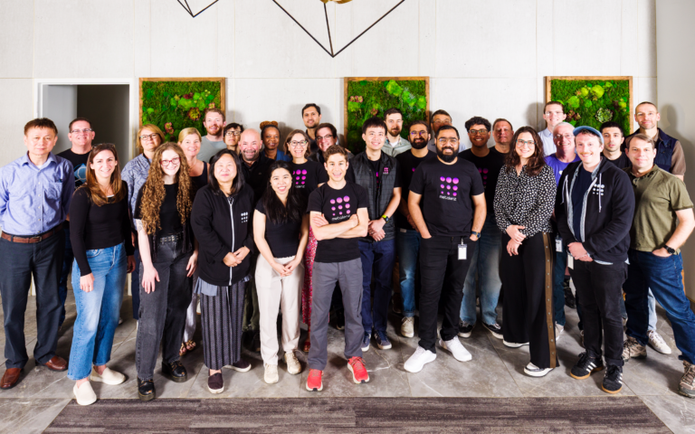
We are on a mission to make smart sensing and new information accessible to billions of people and devices, changing the way people interact with the world. This is our focus and our passion.
We are a team that values critical and creative thinking and encourages new ideas and complex problem solving.
We work hard, we celebrate.
We are proud to have cultivated an environment of constant collaboration and mutual respect- with egos left at the door.
We are a team that values critical and creative thinking and encourages new ideas and complex problem solving.
We work hard, we celebrate.
We are proud to have cultivated an environment of constant collaboration and mutual respect- with egos left at the door.

Built on foundational research from the Capasso Lab at Harvard University.
Built on foundational research from the Capasso Lab at Harvard University.
Metalenz emerged out of stealth in 2021 to become the first company to commercialize meta-optics.
Marking the beginning of this revolutionary optical technology in real-world devices, Metalenz launched meta-optics (metalenses) into consumer devices for the first time in 2022 in a range of consumer devices through its partnership with global semiconductor manufacturing leader STMicroelectronics.






Whether in our smartphones, our car, or medical devices, meta-optics can access whole new sets of information that conventional optics can’t. Our breakthrough technology improves performance with simpler, smaller modules, allowing powerful new sensing capabilities to proliferate to more devices, and impact more lives. We work directly with OEMs, as well as system integrators and image sensing companies.


