Company · About Us
New perception for people and machines.
Metalenz is a fabless semiconductor optics company on a mission to make new information in light accessible to billions of devices. Built on foundational research from the Capasso Lab at Harvard, we are bringing new perception to the next generation of intelligent devices.
300M+
In market today in top consumer brands, multiple foundry partners
Harvard University
Spun out of foundational research in the Capasso Lab, Harvard SEAS
Key Enabler
Deep expertise and IP on foundational tech through full systems solutions
Foundational technology
Multifunctional optics in a single semiconductor layer.
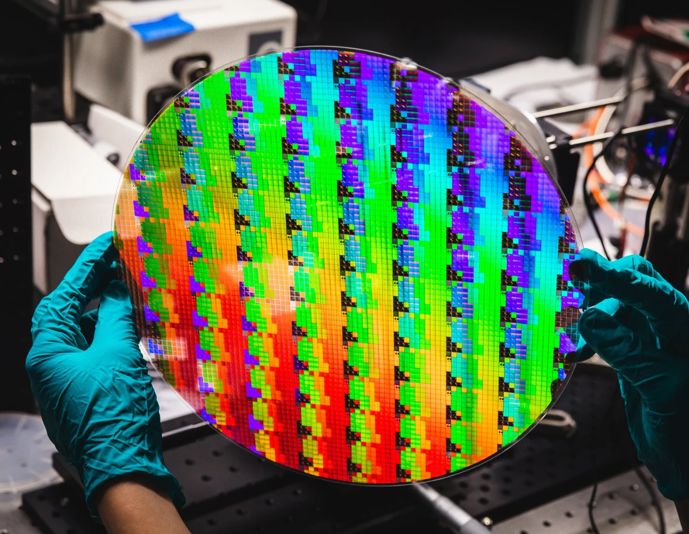
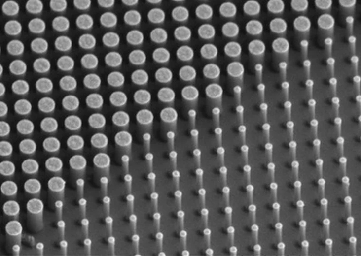
A metasurface is a flat layer of nanostructures, each smaller than a wavelength of light, that bends and sorts light the way a stack of curved lenses does. One Metalenz meta-optic can combine up to five optical functions, removing complexity, shrinking footprint and delivering high performance.

Simplify the system
Multiple optical functions on one surface replace multi-element lens stacks.

Consolidate the supply chain
Optics are made in the same foundries, on the same tools, as the electronics they serve.

Proliferate advanced sensing
Smaller, simpler, cost-efficient modules bring advanced sensing to billions of devices.
Enabling the Metasurface Market
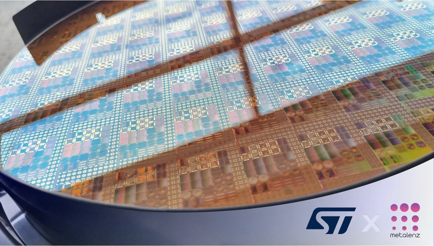
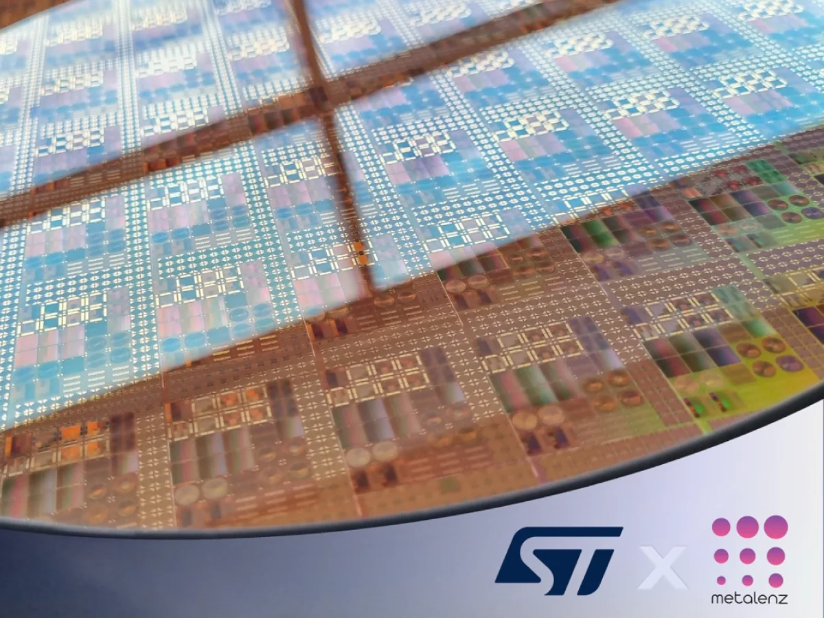
Metalenz emerged from stealth in 2021 as the first company to commercialize metalenses. In 2022, through our partnership with STMicroelectronics, metalenses shipped in consumer devices for the first time. Metasurface components made using Metalenz IP replace existing lens stacks across STMicroelectronics’ FlightSense line for depth mapping. Our collaboration with ST goes beyond replacing lenses: it’s driving an industry shift toward building advanced optics in semiconductor fabs.
More than 300 million Metalenz metasurfaces are in use today across consumer, automotive and industrial markets, in applications from smartphone biometrics, LiDAR and camera assist to robotics, gesture recognition and object detection.
Our evolution
From simplifying optics to full-stack solutions.
Gen 1 · Simplify the optical stack
300M+
Metasurface components deployed
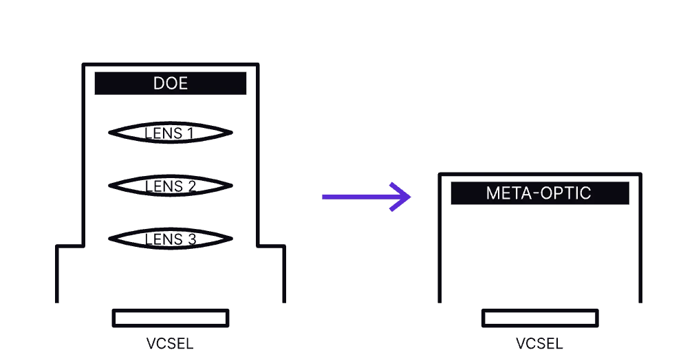
Shipping meta-optics in consumer devices today through licensing and pure-play manufacturing.


Now · System-level design & sensor integration
Full-stack solutions
Designed around the unique capabilities of metasurfaces.
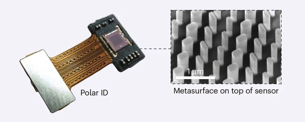
Beginning with trust.
Expanding to insight.
Ecosystem


Platform

First application:
Secure biometrics

The Optical Intelligence Layer
All the information in light. Built for scale.
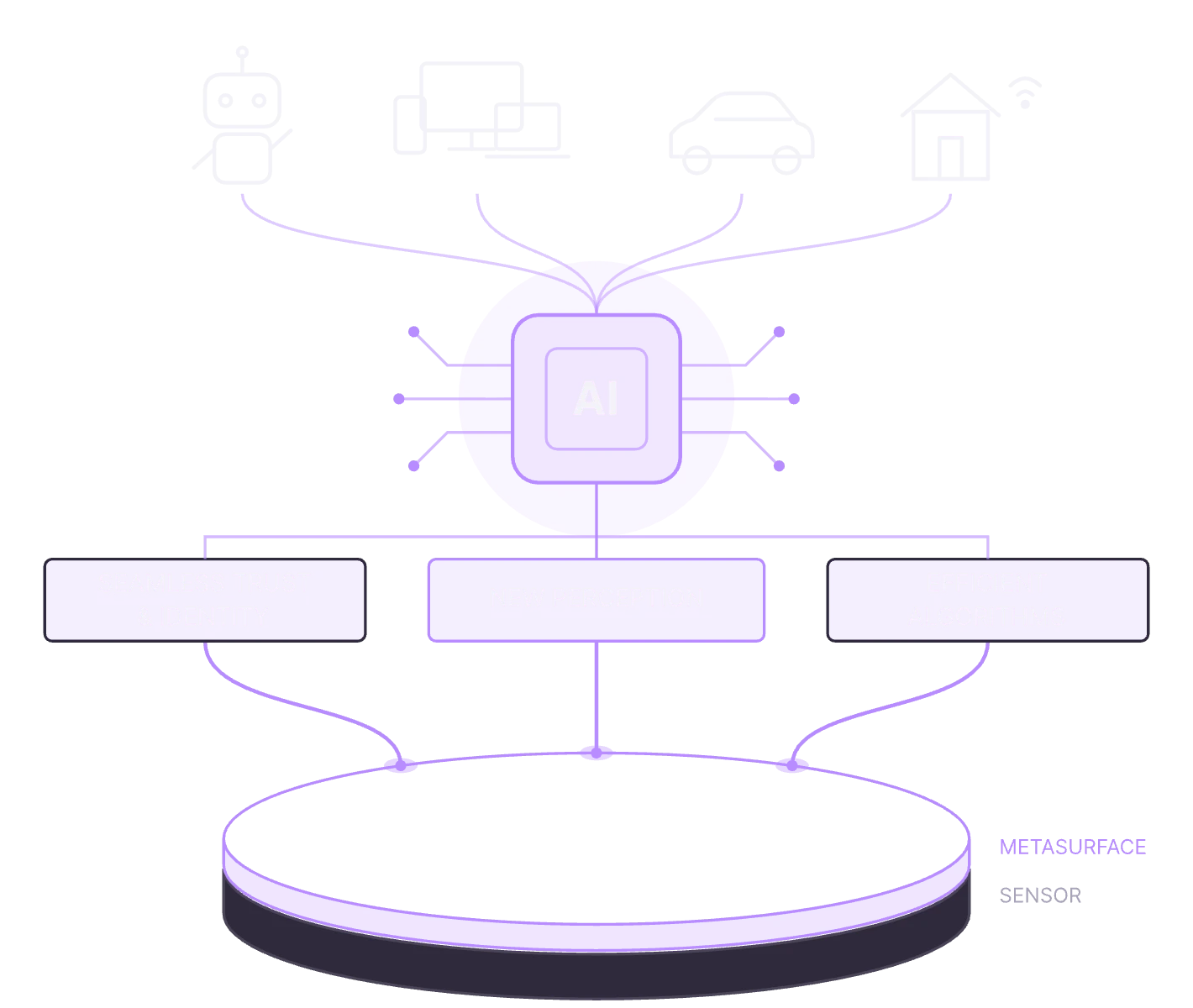
Light carries far more than brightness and color. Polarization reveals shape, surface and material. Phase and the light field encode depth. Conventional cameras record only a fraction of it. Our optical intelligence platforms sort rather than filter light, with a single layer built on the sensor. Our compute stack decodes it to give machines data no conventional camera provides. Better models do more with existing data. New perception at scale creates the data they’ve never had.
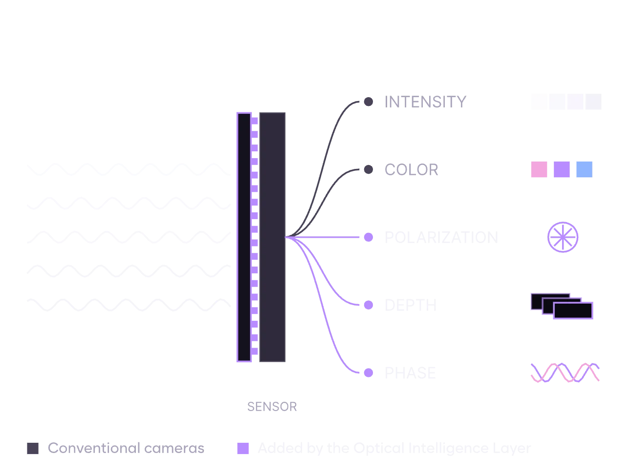
01 · Polarization
Liveness, shape and surface
PolarEyes sorts near-infrared light by polarization on a standard sensor, revealing liveness and material properties for secure authentication, studio-quality relighting and more.
Explore PolarEyes →02 · Color, depth and phase
The visible light field
PxE’s holographic encoder replaces the color filter array, delivering simultaneous color and depth with 2.5x the SNR of Bayer-based cameras.
Explore the PxE platform →03 · Built for scale
Made in the foundry
A single mask layer on existing semiconductor equipment, integrated at wafer level alongside the sensor with no module redesign.
Company highlights
A decade of firsts.
2026
- Metalenz acquires PxE Holographic Imaging, extending optical intelligence to visible-spectrum color and depth
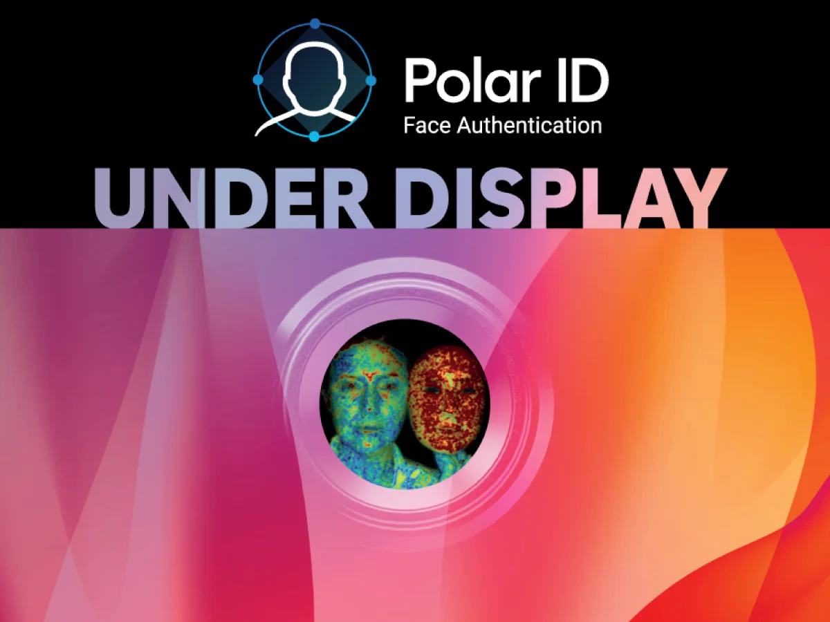
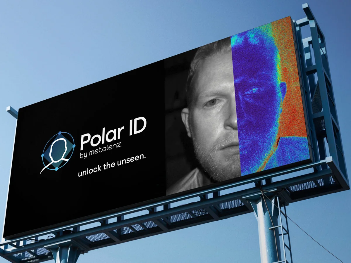
- Polar ID Under Display launches with a live demo at Display Week
- Gen 1 metasurfaces in market top 300 million units
- Polar 3D launches at Mobile World Congress to reimagine selfie relighting
2025
- Polar ID under evaluation with top OEMs
- STMicroelectronics and Metalenz sign a new license agreement to accelerate metasurface optics adoption
- Gen 1 meta-optics pass 140 million units in market
- Product and patent portfolio expands to system-level applications for secure biometrics and simpler 3D depth sensing, including single-element dot pattern projectors
2024
- Polar ID demonstrated live at MWC Barcelona
- Samsung ISOCELL Vizion image sensor confirmed as the light engine for Polar ID

2023
- Metasurface optics launch on the open market in partnership with UMC
- Polar ID announced running on Qualcomm Snapdragon, enabling simple, secure face unlock for smartphones
2022
- World’s first metalens product in mass production with STMicroelectronics
- Portfolio expands to polarization optics with the launch of PolarEyes sensing and Gemini illuminators
- Parts pass module-level reliability for a top OEM
2021
- STMicroelectronics partnership announced
- Orion dot pattern projectors announced
- High-volume, production-ready metalens technology designed into a time-of-flight reference platform
2020
- Single-metasurface imaging invented by Metalenz
- Headquarters moves to downtown Boston

2018
- First high-volume manufacturing demonstration wafers
2016
- Metalenz founded by Rob Devlin and Federico Capasso
- Exclusive license secured to Harvard IP
- First high-quality images captured with metasurfaces at the Cambridge office
Our investors








Awards and recognition
Best of Sensors 2026
Best of Sensors Awards winner

Prism Awards 2026
SPIE Prism Awards winner

Optica 2025
Kevin P. Thompson Optical Design Innovator Award, Rob Devlin

AI Breakthrough 2024
Best Overall Biometrics Solution

EE Times 2024
Silicon 100: Startups Worth Watching

Prism Awards 2023
SPIE Prism Awards winner

Laser Focus World 2022
Innovators Awards Platinum Honoree

The FIRE Awards 2022
BostInno Blazer: Consumer Goods
Latest news